
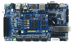


MYD-C7Z015 Development Board
High Performant Boad Dual-core ARM Cortex-A9
The MYD-C7Z015 development board, designed by MYIR, features the Xilinx XC7Z015 (Z-7015) Dual-core ARM Cortex-A9 Processor and Xilinx 7-series FPGA logic. With PCIe and SFP interfaces, it suits various high-speed devices for applications like Industrial Automation, Medical Equipment, and Aerospace.
Powered by the MYC-C7Z015 CPU Module, the board integrates core components including Zynq-7015 processor, DDR3 SDRAM, eMMC, and more. With enhanced programmable functions, it offers versatile applications, supported by rich peripherals like RS232, USB, Gigabit Ethernet, HDMI, and PCIe interfaces.
The MYD-C7Z015 development board is preloaded with Linux and delivered with necessary cable accessories. It is a high-performance and low-cost development platform for evaluation and prototype based on Xilinx Zynq-7000 All Programmable SoC family.
Accessories:
12V/5A Power Supply
Features:
Mechanical Parameters
| Dimensions: 190mm x 110mm (base board), 75mm x 55mm (CPU Module) | |
| PCB layers: 4-layer design (base board), 12-layer design (CPU Module) | |
| Power supply: 12V/0.5A (base board), 5V/0.5A (CPU Module) | |
| Working temp.: -40~85 Celsius (industrial grade) |
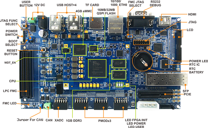
Xilinx XC7Z015-2CLG485I (Zynq-7015)
- Four high-speed SerDes transceivers up to 6.25Gbps
- Four PCIe Gen2 hardened, integrated IP blocks
- 766MHz ARM® dual-core Cortex™-A9 MPCore processor (up to 866MHz)
- Integrated Artix-7 class FPGA subsystem with 74K logic cells, 46,200 LUTs, 160 DSP slices
- NEON™ & Single / Double Precision Floating Point for each processor
- Supports a Variety of Static and Dynamic Memory Interfaces
Memory:
| 1GB DDR3 (2 x 512MB, 32-bit) |
| 4GB eMMC |
| 1GB DDR3 (2 x 512MB, 32-bit) |
Peripherals and Signals Routed to Pins
| 10/100/1000M Ethernet PHY | |
| One USB PHY | |
| External watchdog | |
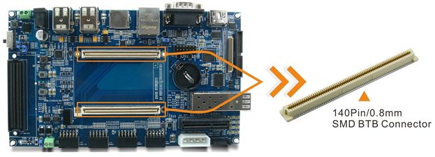
| Three LEDs | - One blue LED for power indicator - One red LED for FPGA program done indicator - One green user LED Two 0.8mm pitch 140-pin board-to-board expansion connectors bring out below signals: - One Gigabit Ethernet - One USB OTG 2.0 - Up to two Serial ports - Up to two I2C - Up to two CAN BUS Serial ports, I2C and CAN signals will be reused in PS part, or implemented through PL pins - One SPI (can be implemented through PL pins) - ADC (one independent differential ADC, 16-channel ADC brought out through PL pins) - One SDIO - Bank 13 (PL I/O configurable as up to 18 LVDS pairs and 1 single-ended I/O or 37 single-ended I/O) - Bank 34 (PL I/O configurable as up to 24 LVDS pairs and 2 single-ended I/O or 50 single-ended I/O) - Bank 35 (PL I/O configurable as up to 24 LVDS pairs and 2 single-ended I/O or 50 single-ended I/O) - Bank 112 (4 GTP serial transceivers, 2 reference clock input) |
PS Unit
| Four USB 2.0 Host ports (through USB Hub) |
| One RS232 (DB9 port) |
| One TF card slot (bootable) |
| One CAN interface |
| One 10/100/1000M Ethernet |
| One 2.54mm pitch 14-pin JTAG interface (PS, PL reused) |
| Battery backed RTC |
| One User Button (One I2C, can be connected to LCD and Resistive Touch Screen) |
| Jumpers - One for booting selection from TF card or QSPI - One for JTAG selection for using PS and PL reused or independent JTAG configured through PL pins - One for selection if adding FMC module to JTAG |
PL Unit
| One XADC interface |
| One Xilinx standard LPFMC interface |
| One HDMI interface (16-bit YCrCb, support 1080p display, do not support audio) |
| LCD/Touch screen interface (16-bit RGB, signals reused with HDMI, supports resistive and capacitive touch screen) |
| Two LEDs (one for FMC module detection, one for power indicator) |
| Three-channel PMoD |
| One SFP transceiver module with RJ45 interface (SFP-GE-T module, up to 1000Mbps) |
| One PCIe interface |
| OS Support Linux 5.4.0 |
The MYD-C7Z015 Base Board (MYB-C7Z015)
MYD-C7Z015 Base Board (MYB-C7Z015)